Summary:
- Intel’s lifetime deal value for its IFS foundry business is now over $10 billion, indicating strong growth potential in advanced packaging.
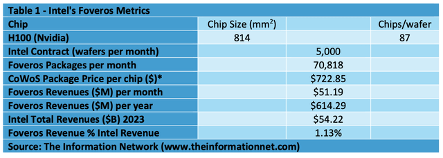
- Intel will supply TSMC with 5,000 Foveros wafers per month, generating potential packaging revenues of $614.29 million per year.
- Intel’s Foveros packaging technology is expected to generate 5% of the company’s overall revenues of $68 billion in 2026.

koya79/iStock via Getty Images
IFS Foundry Business a “Diamond in the Rough”
At Intel’s (NASDAQ:INTC) Q4 2023 earnings call, CEO Gelsinger remarked:
“To support our growing demand, just yesterday, we opened Fab 9 in New Mexico, marking a milestone for high-volume 3D advanced packaging manufacturing. The momentum in advanced packaging is very strong and is another facet of our foundry strategy, which is clearly benefiting from the surge of interest in AI. With leadership technology and available capacity, our opportunity set continues to grow. In total, across wafer and advanced packaging, our lifetime deal value for IFS is now over $10 billion, more than doubling from the $4 billion we provided in our last update.”
Currently, $10 billion represents less than Intel’s $15 billion in revenues for Q4. But in this article, I show how CEO Gelsinger is underrepresenting its potential.
My favorite writer, Anton Shilov noted in an article for Tom’s Hardware entitled “Nvidia reportedly selects Intel Foundry Services for GPU packaging production — could produce over 300,000 H100 GPUs per month.”
TSMC recently increased its CoWoS production capacity from 12,000 to 15,000 wafers per month, which will double in 2024, at which point GPU supplier Nvidia (NVDA) should account for 40% of TSMC’s CoWoS production capacity.
But TSMC is capacity limited because of the strong demand from Nvidia chips like the A100 and H100. According to the article, Intel will supply TSMC with 5,000 Foveros wafers per month.
In Table 1, I present my analysis of the benefit to Intel from this arrangement. Based on an Nvidia H100 GPU chip size of 814 mm2, a total of 87 H100 chips can be made, assuming 100% yield, the 5,000 wafers per month can make 70,818 Foveros packages.
This analysis is based on my July 11, 2023, Seeking Alpha article entitled “Taiwan Semiconductor’s CoWoS Package A Game Changer For Generative AI,” where I calculated the price of TSMC’s CoWoS package of $722.87. At that price, Intel can generate $51.19 million per month or $614.29 million for a year.
That represents just 1.13% of Intel’s $54.22 billion in revenues for 2023.

The Information Network
Intel announced in late January 2023 that Fab 9 had begun operations at its Rio Rancho site in New Mexico. The $3.5 billion production facility was built to package chips using Foveros 3D technology and is one of Intel’s first fabs dedicated solely to advanced packaging technologies.
Intel employs its Foveros 3D technology in crafting the latest Core Ultra ‘Meteor Lake’ processors for client applications and Ponte Vecchio GPUs for AI and HPC tasks. With Intel and its Intel Foundry Services clients increasingly adopting multi-chiplet designs, the application of Foveros 3D is set to rise significantly in the future.
Details on Packages
TSMC’s CoWoS Package
As a background, Taiwan Semiconductor’s (TSMC) (TSM) CoWoS (Chip-on-Wafer-on-Substrate) is an advanced packaging technologies designed to address the limitations of traditional 2D chip stacking methods using a glass interposer.
TSMC first developed its CoWoS package for advanced chips in 2012 and combined with High Bandwidth Memory (“HBM”) in 2016. The explosion of generative AI technology such as ChatGPT has been a catalyst for growth of TSMC’s CoWoS chip packages that now reaches 7% of total revenues.
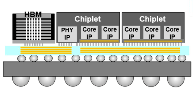
Chart 1 is a diagram of TSMC’s CoWoS (Chip on Wafer on Substrate) package. CoWoS allows the integration of multiple chips or dies onto a single package. This enables the combination of different types of chips, such as processors, memory, and graphics, into a single package, resulting in improved performance, reduced power consumption, and smaller form factors.

AMD
Chart 1
Multiple chips are stacked vertically using through-silicon vias (TSVs) and interconnected with micro-bumps. This stacking approach enables shorter interconnect lengths, reduces power consumption, and improves signal integrity compared to traditional 2D packaging.
By integrating HBM with CoWoS, the memory dies can be placed closer to the processor, reducing the interconnect length and enabling even faster and more efficient data transfer between the processor and memory. This increased memory bandwidth is particularly beneficial for memory-intensive applications such as artificial intelligence, high-performance computing, and graphics processing.
Chiplet technology, as illustrated above in Chart 1, is an approach that involves dividing a large monolithic chip into smaller functional blocks called chiplets. Each chiplet focuses on a specific function or subsystem, such as a processor core, memory controller, or I/O interface. These chiplets can be designed and manufactured independently using different process technologies, and then assembled and interconnected on a package or an interposer. The chiplets are connected through high-speed interconnects, such as micro-bumps or wire bonds.
Intel’s Foveros
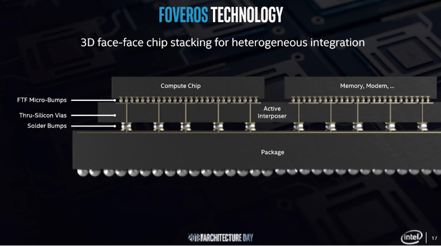
Intel’s Foveros is a pioneering 3D packaging technology that represents a significant leap in semiconductor manufacturing and design. Introduced in 2018, Foveros enables the vertical stacking of compute dies and logic chips, allowing for a level of component integration and form factor reduction previously unachievable with traditional 2D packaging methods. This technology is part of Intel’s broader strategy to overcome the limitations of Moore’s Law by innovating in the way components are integrated and interconnected, rather than just shrinking transistor sizes. Foveros is illustrated in Chart 2.

Intel
Chart 2
Comparisons between CoWoS and Foveros
Similarities:
1. 3D Stacking:
Both Foveros and CoWoS enable 3D stacking of different semiconductor components, allowing for improved performance and power efficiency.
2. Heterogeneous Integration:
Both technologies support the integration of chips made using different process technologies, facilitating the creation of more complex and specialized systems.
Differences:
1. Company and Ecosystem:
Intel’s Foveros: Developed by Intel, Foveros is an in-house packaging technology primarily used in Intel’s own processors and chips.
TSMC’s CoWoS: CoWoS is a packaging technology offered by TSMC (Taiwan Semiconductor Manufacturing Company) as part of its foundry services, allowing multiple companies to utilize the technology for their products.
2. Design Flexibility:
Intel’s Foveros: Provides flexibility in designing heterogeneous chips with different functionalities, optimizing performance and power consumption.
TSMC’s CoWoS: Offers flexibility in integrating different chips on the same package, allowing for diverse combinations of components.
3. Implementation in Products:
Intel’s Foveros: Implemented in products like Lakefield processors, featuring a mix of high-performance and low-power cores for ultra-thin laptops and foldable devices.
TSMC’s CoWoS: Used in various applications, including high-performance computing, networking, and advanced memory solutions, depending on the needs of TSMC’s diverse customer base.
4. Target Applications:
Intel’s Foveros: Initially focused on mobile and low-power applications, with plans to expand into client, server, graphics, and AI accelerators.
TSMC’s CoWoS: Widely used across various market segments, including high-performance computing, networking, and data center applications.
5. Interconnect Technology:
Intel’s Foveros: Utilizes advanced interconnect technologies such as through-silicon vias (TSVs) and micro-bumps to enable vertical stacking.
TSMC’s CoWoS: Uses silicon interposers to connect chips in a 3D configuration, providing high bandwidth and low-latency communication.
6. Market Accessibility:
Intel’s Foveros: Primarily available in Intel’s own products, limiting accessibility to external companies.
TSMC’s CoWoS: Offered as part of TSMC’s foundry services, making it accessible to a broad range of semiconductor companies worldwide.
Investor Takeaway
Intel is scheduled to host an event on February 21 to unveil its foundry roadmap. Currently, its list encompasses Intel’s advanced product lineup, including the Ponte Vecchio compute GPU for high-performance computing, the Sapphire Rapids and Sapphire Rapids HBM processors tailored for data centers and supercomputers, and the forthcoming client CPUs: Meteor Lake, Arrow Lake, and Lunar Lake.

Intel
Chart 3
According to a report by The Information Network titled “High-Density Packaging (MCM, MCP, SIP, 3D-TSV): Market Analysis and Technology Trends,” revenue from advanced-chip-packaging is forecasted to increase from $44 billion in 2023 to $79 billion by 2028. In comparison, the traditional chip packaging market, valued at approximately $47 billion last year, is expected to grow to $57 billion by the same year. Consequently, the entire chip packaging market is anticipated to achieve a total value of $136 billion by 2028.
According to the above report from The Information Network, TSMC will generate $9.31 billion in 2024. Just the contract between TSMC and Intel will generate $615 million in packaging revenues.
But based on Intel’s roadmap above and TSMC’s historic CoSoW growth trajectory, I estimate Intel’s Foveros packaging will generate 5% of the company’s overall revenues of $68 billion in 2026. That would equate to packaging revenues of $3.4 billion.
That figure would include not only Intel’s internal chips, but those for its foundry customers. Already the company has signed on five packaging customers. Intel CEO Gelsinger commented in the earnings call:
“During the quarter, we captured three additional advanced packaging design wins, bringing the total to five in 2023, with the majority of revenue starting in 2025.”
Based on Intel’s recent earnings call and guidance, I rate the company a Hold. Its advanced packaging will be a game changer, but verification of TSMC’s off-loading plan remains to be verified and important for 2024. For 2025 and beyond, packaging will be a strong tailwind for its Foundry business.
Importantly, the technology learning curve on Foveros on “TSMC’s dime” will lift the company from packaging its own chips, when available, to being a full-fledged advanced packaging foundry for other AI semiconductor companies searching for a packaging house as TSMC remains in short supply.
But the opportunity goes beyond that. TSMC’s small node capacity is also under allocation, particularly for new customers as it focuses on its existing customers such as Apple (AAPL).
Fabless companies that don’t make their own chips prefer a “one-stop shop.” Most go to TSM, which makes the chips and then packages them. As Intel ramps its packaging foundry business, it will naturally be an opportunity for Intel to fabricate the chips for these companies as well.
The Intel-TSM deal will generate $600 million for Intel based on just 5,000 wafers per month for the 1-year period. Hyperscalers will be the prime customer for Intel. These include Alphabet (GOOGL) and Meta (META). This could bode well, as Intel’s Data Center and AI (“DCAI”) business fell another 10% year-over-year in Q4 to $4 billion, and ended down 20% for full-year 2023 to $15.5 billion.
But based on Intel’s roadmap above and TSMC’s historic CoSoW growth trajectory, I estimate Intel’s Foveros packaging will generate 5% of the company’s overall revenues of $68 billion in 2026. That would equate to packaging revenues of $3.4 billion.
Analyst’s Disclosure: I/we have no stock, option or similar derivative position in any of the companies mentioned, and no plans to initiate any such positions within the next 72 hours. I wrote this article myself, and it expresses my own opinions. I am not receiving compensation for it (other than from Seeking Alpha). I have no business relationship with any company whose stock is mentioned in this article.
Seeking Alpha’s Disclosure: Past performance is no guarantee of future results. No recommendation or advice is being given as to whether any investment is suitable for a particular investor. Any views or opinions expressed above may not reflect those of Seeking Alpha as a whole. Seeking Alpha is not a licensed securities dealer, broker or US investment adviser or investment bank. Our analysts are third party authors that include both professional investors and individual investors who may not be licensed or certified by any institute or regulatory body.
This free article presents my analysis of this semiconductor equipment sector. A more detailed analysis is available on my Marketplace newsletter site Semiconductor Deep Dive. You can learn more about it here and start a risk free 2 week trial now.
