Summary:
- Nvidia Corporation’s Q3 guidance disappointed due to a delay in the Blackwell AI chip, caused by a mask issue affecting chip yield, not design flaws.
- Despite the delay, Nvidia’s revenue growth remains strong, with a projected 79% y/y growth for Q3 and significant Blackwell revenue expected in Q4.
- Blackwell’s advanced packaging technology is ambitious but proven, and the chip promises substantial AI performance improvements over competitors like AMD’s MI300X.
- Nvidia Corporation is poised to dominate the future $2 trillion data center market, with an estimated $955 billion in cumulative revenue from fiscal 2025 to 2029.
Antonio Bordunovi
Although Nvidia Corporation (NASDAQ:NVDA) reported fiscal 2025 Q2 results well above guidance, investors were disappointed with the guidance for fiscal Q3. This was mainly due to the delay in Nvidia’s next-generation AI accelerator chip for the data center, dubbed Blackwell. Rumors have swirled around the delay, and some incorrect or misleading information about Blackwell has been reported. In this article, I take a closer look at the Blackwell delay and what it means for Nvidia’s results in fiscal Q3 and Q4.
My take on the Blackwell delay
On August 2, The Information released a report that Nvidia’s Blackwell would be delayed by at least a quarter due to unspecified “design flaws.” Normally, when one hears about the design flaws of a chip, logic design problems or bugs come to mind. But Nvidia management made clear that this was not the case during their fiscal Q2 results conference call.
Instead, there was an issue with a mask that impacted chip yield, said CFO Colette Kress:
Hopper demand is strong and Blackwell is widely sampling. We executed a change to the Blackwell GPU mask to improve production yields. Blackwell production ramp is scheduled to begin in the fourth quarter and continue into fiscal year ’26.
Presumably, the chip yield affects the number of good chips resulting from each silicon wafer fabricated by foundry partner TSMC (TSM). CEO Jensen Huang reiterated that there was nothing wrong with the functional design of the chip. The mask change did not change the functional logic of the chip.
Developing the mask to implement a given layer of circuitry on an advanced chip has become an enormously complex process. This is because at the extreme ultraviolet wavelength of 13.5 nm, diffraction effects and optical distortion mean that the light pattern produced on the chip doesn’t look like the mask.
Optical physicists try to work backwards from the desired pattern to predict what the mask should look like, depending on the EUV machine and other factors. The process is computationally intensive, and TSMC has invested in an Nvidia supercomputer to perform what is called “computational lithography.”
The process isn’t perfect, and the actual pattern produced by a mask may not match the computational lithography prediction. Since the issue is one of yield, this is probably what happened in the case of Blackwell, and why it’s going to take several months to find a more optimal mask solution and begin mass production.
Asa Fitch’s article in the WSJ reported on the Blackwell delay:
Nvidia hasn’t detailed the nature of the issue. But analysts and industry executives say its engineering challenges stem mostly from the size of the Blackwell chips, which require a significant departure in design.
I disagree with this interpretation. Nvidia has been making its flagship GPU accelerators (such as Hopper), at TSMC’s reticle limit, for years. This sets the maximum physical size of a chip that TSMC can produce using EUV lithography machines produced by ASML Holding (ASML).
Blackwell does consist of two such chips, but the process to make each is essentially unchanged from Hopper. Blackwell is fabbed, using basically the same TSMC N4 process as Hopper. Fitch continues:
Instead of one big piece of silicon, Blackwell consists of two advanced new Nvidia processors and numerous memory components joined in a single, delicate mesh of silicon, metal and plastic.
The manufacturing of each chip has to be close to perfect: serious defects in any one part can spell disaster, and with more components involved, there is a greater chance of that happening.
Once again, I have a different interpretation. The fact that the package consists of two chips doesn’t make the chips harder to make. Each chip already needs to be “close to perfect.” The added complexity is in packaging, not in making the silicon. And it certainly doesn’t have anything to do with the mask issue.
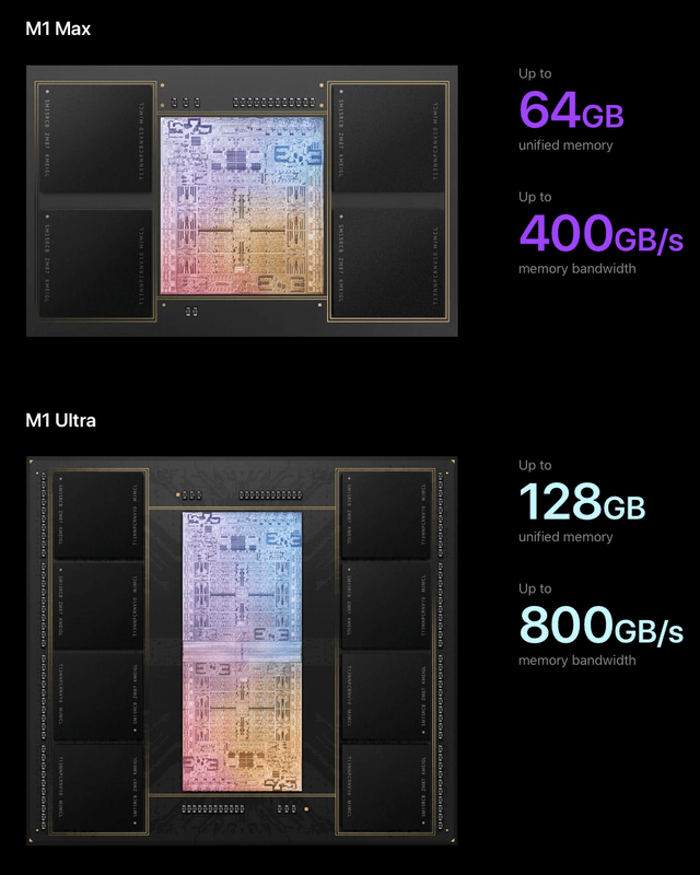
As I pointed out in my investing group article on the Blackwell debut back in March, the approach had already been pioneered by Apple (AAPL) and TSMC in their M-series Ultra processors.
The Ultra chips consist of two M-series Max chips joined edge-to-edge, as shown for the M1 Ultra:
TSMC seems to be making a similar packaging approach available to Nvidia for Blackwell. This would indicate that the two Blackwell chips are identical and therefore no more difficult to make than Hopper.
How Blackwell compares with AMD’s MI300X, MI325X
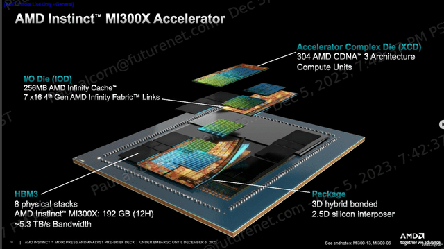
The strongest competition to Nvidia’s data center AI accelerators is posed by Advanced Micro Devices (AMD) with its AMD Instinct line of GPU accelerators. The Blackwell approach is certainly less complex than what AMD uses for its flagship data center accelerator, the MI300X, which uses multiple chiplets and interposers:
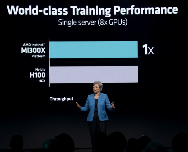
The MI300X has been hailed as an “Nvidia Killer,” yet when AMD launched it, AMD could only claim performance parity in AI training to the Hopper H100:
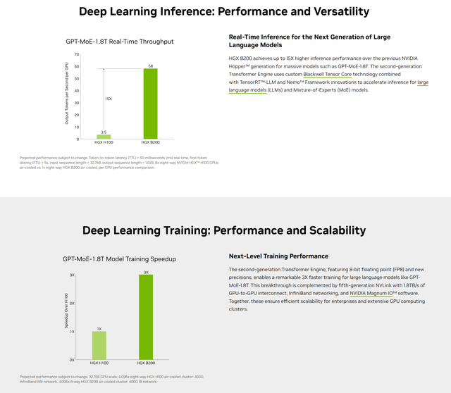
However, Nvidia claims a huge performance improvement for Blackwell over Hopper H100 in both training and inference:
Nvidia has also published some early results on MLCommons, which tabulates AI benchmarks for systems that run MLPerf tests. In the llama2-70B inference benchmark, the Blackwell B200 bested the MI300X by a factor of 3.67.
In calendar Q4, AMD is expected to release the MI325X, which is basically identical to the MI300X but with more memory and higher memory bandwidth. The memory improvements will help performance, but will probably not close the gap with Blackwell.
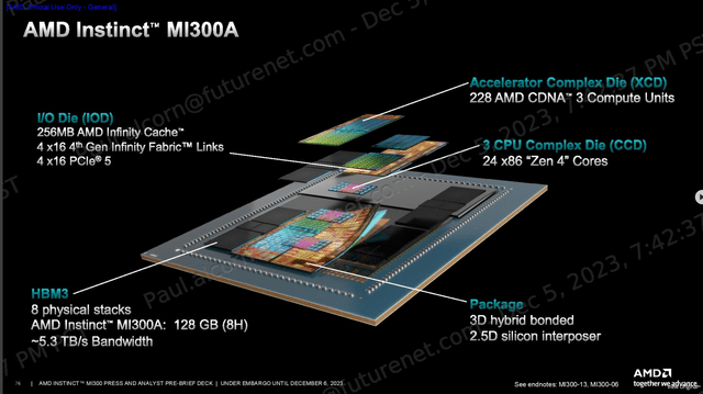
The MI300 series chips are powerful accelerators, but they fall short of Nvidia in AI performance because they were never really meant for AI. Originally, the MI300A was intended to power the El Capitan supercomputer of Lawrence Livermore. This was what AMD refers to as an “APU,” an SOC with CPU and GPU cores:
Following the announcement of the APU for El Capitan in August 2022, AMD announced the pure GPU MI300X variant in June 2023.
The financial impacts of the Blackwell delay
Nvidia didn’t specify how much wastage there was due to the Blackwell mask problem, but apparently some wafers already bought and paid for from TSMC had to be scrapped. This was disclosed as a contributor to a sequential decline of gross margin from 78.35% in fiscal Q1 to 75.15% in Q2.
With production Blackwell chips not scheduled to ship until fiscal Q4, Q3 guidance was muted but still very respectable with 79% y/y revenue growth and net income y/y growth of 84%. But it just couldn’t compare with the huge growth rates of quarters past.
And it couldn’t possibly. Fiscal 2024 Q3 was when generative AI really took off, and company revenue grew by over 200%. This “law of large numbers” effect merely means that percent changes are going to get smaller, even if the magnitude of the revenue change stays the same.
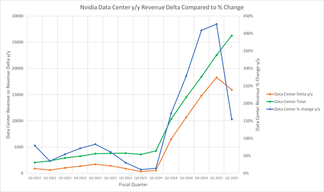
We can see this effect in the following chart:
The Data Center Delta is the y/y absolute difference in revenue. In fiscal 2025 Q1, even though the delta had continued to get larger, the percent change leveled off. The y/y percent change plunged in fiscal Q2, even though the delta decreased only slightly from fiscal Q1.
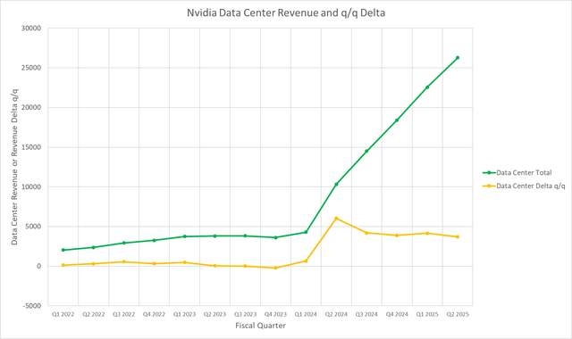
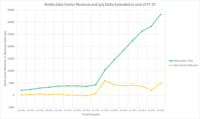
The expectation that revenue growth should be always proportionate to revenue is probably not realistic. Allow me to suggest a better way to look at Nvidia’s Data Center revenue trajectory. Since Q2, that trajectory has been nearly a straight line:
The slope of the line can be approximated as the difference between current quarter revenue and the previous quarter, divided by 1 quarter of time. In effect, the slope is just given by the sequential revenue difference or delta, shown plotted in yellow.
Where the line is straight or nearly so, the slope is constant. The slope is greatest in fiscal 2024 Q2, when the AI boom began for the Data Center segment. But the constant slope in the following quarters implies that the revenue growth was sustainable.
Then came the Blackwell delay, and the midpoint of revenue guidance implies a decreased rate of growth in the Data Center, as shown below:
If the slope of the line were expected to continue to fall, this would be very concerning. But there’s no reason to expect that it will. Nvidia expects demand for Hopper H200 to continue to grow into Q4, while Blackwell adds additional revenue to the data center. Kress said:
In Q4, we expect to ship several billion dollars in Blackwell revenue. Hopper shipments are expected to increase in the second half of fiscal 2025. Hopper supply and availability have improved. Demand for Blackwell platforms is well above supply, and we expect this to continue into next year.
This is reflected in my projection for fiscal Q4 Data Center revenue and the recovery of the slope line.
Investor takeaways: Blackwell to propel growth
The production snag that Blackwell hit was nothing unusual in advanced semiconductor fabrication and would probably have gone unnoticed were it not for the accelerated schedule for Blackwell’s release. Previous releases have been far more leisurely.
The delay says nothing about the fundamental viability or producibility of the chip. The packaging technology used for Blackwell is ambitious but by no means new. And the chip represents another quantum leap in AI performance and computational efficiency.
The AI industry needs that efficiency to keep from draining away all the world’s electrical generating capacity. We’re in the early stages of a roughly $2 trillion revamp of the world’s data centers.
At Nvidia’s 2024 GPU Technology conference in March, during a Q&A with analysts, Huang estimated that the data center infrastructure spending rate was about $250 billion per year. Depending on how long the spending rate is sustained, that would be about $1-2 trillion in spending over the next ten years.
Also during Q&A, Vivek Arya of Bank of America bounded the total addressable market as being in the $1-2 trillion range. I believe that with the growth of sovereign AI, where countries invest in domestic AI infrastructure, that we’ll be at the upper bound of that range by the end of the decade.
This revamp is being pursued not merely for the sake of AI, but for purposes of greater efficiency as data center operators turn to GPU acceleration for a wide variety of workloads besides AI. These include big data analytics, video and game streaming, metaverse applications, etc.
One of the advantages of GPU accelerators over special purpose ASICs is versatility, the ability to do other useful things besides AI. This is why I consider AMD the strongest competitor.
Do I think that Nvidia will scoop up all the $2 trillion data center opportunity? No, I don’t. In addition to AMD, Nvidia will face competition from in-house developed AI accelerators such as Google’s (GOOG) (GOOGL) TPU, and chips developed by Amazon (AMZN), and even, as was recently disclosed at WWDC, by Apple.
I’m currently making a conservative assumption that Nvidia’s Data Center cumulative revenue from fiscal 2025 through 2029 will be $955 billion, or less than half of the projected opportunity. But even then, I expect Nvidia to be the dominant player in the space. I remain long Nvidia stock and rate it a Buy.
Analyst’s Disclosure: I/we have a beneficial long position in the shares of NVDA, AAPL, TSM either through stock ownership, options, or other derivatives. I wrote this article myself, and it expresses my own opinions. I am not receiving compensation for it (other than from Seeking Alpha). I have no business relationship with any company whose stock is mentioned in this article.
Seeking Alpha’s Disclosure: Past performance is no guarantee of future results. No recommendation or advice is being given as to whether any investment is suitable for a particular investor. Any views or opinions expressed above may not reflect those of Seeking Alpha as a whole. Seeking Alpha is not a licensed securities dealer, broker or US investment adviser or investment bank. Our analysts are third party authors that include both professional investors and individual investors who may not be licensed or certified by any institute or regulatory body.
Consider joining Rethink Technology for in depth coverage of technology companies such as Apple.
