Summary:
- Intel is restructuring its development teams based on technology modules, aiming to reduce delays in technology rollouts and drive innovation in next-generation chips.
- Intel’s RibbonFET design, similar to TSMC’s gate-all-around transistors, and adoption of PowerVia for signal and power separation contribute to improved switching speed and miniaturization.
- Intel plans to introduce Intel20A as the successor to Intel 3, offering a 15% performance improvement with RibbonFET and PowerVia.
- Intel’s internal foundry model and IDM 2.0 strategy aim to enhance competitiveness, attract external customers, and drive cost savings. The company plans to achieve $8-$10 billion in cost savings by 2025.
Leon Neal
Investment Thesis
Intel Corporation’s (NASDAQ:INTC) retirement from chip generation-based development organizations and its revamped development approach could lead to an accelerated push for next-generation chip innovation. The company’s focus on technology modules, such as transistors and power supply, along with advancements like RibbonFET and PowerVia, may streamline technology rollouts and drive sales for chipmaking equipment suppliers.
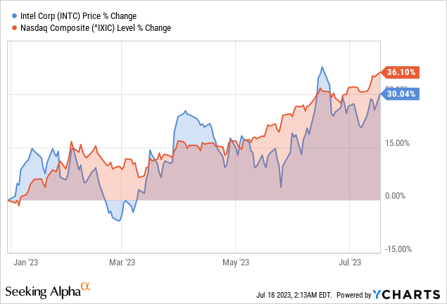
Since I called the bottom in Intel’s stock at $25.54, when trading around its Book Value of $24.20 per share, INTC has gained nearly 37%, in line with the Nasdaq Composite’s performance year-to-date. Following the 52-week drop, I have averaged down my position, turning profitable on the way up. However, following the recent momentum, INTC is a buy, with any pullback around or preferably below $30 moving the stock back to the strong buy rating.
Intel Accelerating Shift To Next-Gen CPUs
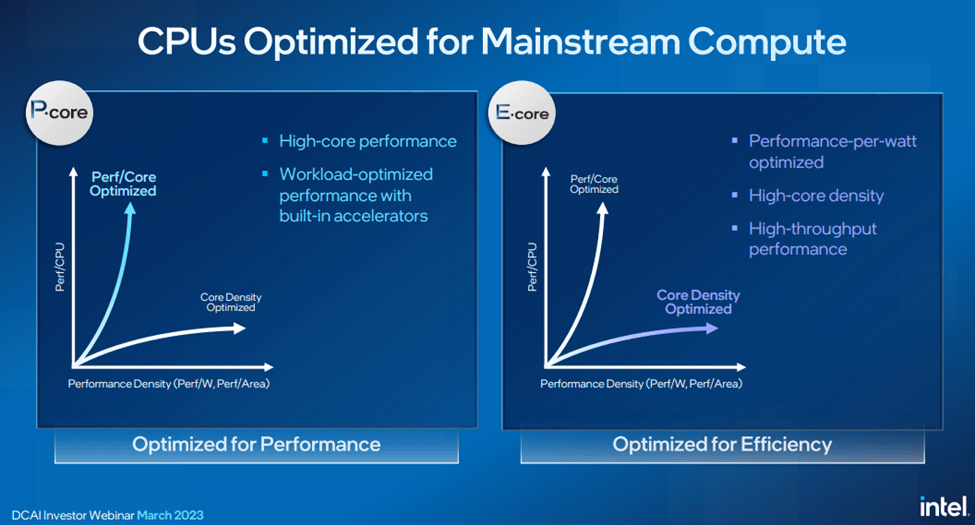
Intel might accelerate its push to innovate next-generation chips due to its retirement from chip generation-based development organizations. In its revamped development approach, Intel builds teams based on technology modules, such as transistors, power supply, and signal lines. This could reduce delays in technology rollouts. The structural design of its RibbonFET, similar to TSMC’s gate-all-around transistors, could help shorten the switching speed and enable miniaturization.
Intel is likely the first adopter of PowerVia, which minimizes signal noise and drops in the power supply’s voltage by separating the signal and power lines. After setbacks in technological advancements in recent years, Intel’s return to developing innovative tech might drive sales of chipmaking equipment and material suppliers.
Intel plans to introduce Intel20A as the successor generation to Intel 3 as it expects the chip world to enter the angstrom (10 billionths of a meter) age. Intel20A aims to offer a 15% improvement in performance compared to Intel 3 by introducing two new technologies: a newly-designed RibbonFET transistor structure and PowerVia, a backside power-delivery network (BS-PDN).
The commercial launch of backside power-delivery networks (BS-PDNs), an essential technology for improving next-generation chip performance, is proceeding apace and is possible within 1-2 years. While other major global chipmakers, such as Samsung Electronics Co., Ltd. (OTCPK:SSNLF) and Taiwan Semiconductor Manufacturing Company Limited (TSM), also plan to adopt BS-PDN, Intel is among the most active in promoting the technology.
The conglomerate plans to adopt BS-PDN in a processor using Intel20A technology scheduled for release in 2024. TSMC and Samsung plan to adopt BS-PDN in their 2-nanometer generation products. Finally, Intel can leverage BS-PDN, or Backside Power Delivery Network, to improve power efficiency and performance in their microprocessors. BS-PDN reduces power loss during transmission, optimizing power distribution and minimizing leakage.
To reduce manufacturing risks amid the simultaneous introduction of two new technologies, Intel plans to focus production on PowerVia before manufacturing RibbonFET transistors. Intel expects to finish preparing the groundwork for volume production of Intel20A by 2024 before introducing a CPU using 20A technology for client PCs under the codename Arrow Lake.
The closing act of Intel’s roadmap of five generations of chip-technology development in four years is Intel18A, which aims for a 10% improvement in performance over Intel20A. The company’s planned launch of data center CPU Clearwater Forest in 2025 and client PC CPU Lunar Lake in 2H25 or 2026 will likely utilize its 18A technology, for which production is expected to be ready by 2024.
Given Intel’s plan to offer 18A technology to clients using its foundry service, mastering 18A might impact the company’s CPU business and its foundry division. Chipmaking tools and material suppliers likely find TSMC’s dominance in producing advanced chips a barrier to sales growth. Lastly, healthy competition among TSMC, Intel, and Samsung could increase demand for advanced chip gear and materials.
Intel’s Investor Webinar 2023
IDM 2.0 Model: Unlocking Cost Savings & Fabless Efficiency
The Foundry Model Investor Webinar mainly explained the inner workings of the new IDM model accounting (starts Q1’24) and left any Intel Foundry Services (IFS) customer announcements to another webinar later in the year. The company highlighted that the Intel PDK for 18A is still where they would like it to be.
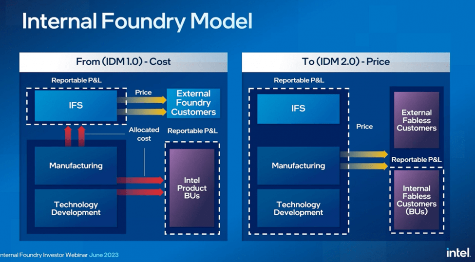
Under the new IDM 2.0 model, business units (BUs) will interact with IFS like fabless companies. They will be charged market rates for various services, including wafers, expedites, samples, and tests. This approach aims to prompt BUs to reduce unnecessary costs, such as expedites, which have been occurring at a higher rate than peers and have resulted in an 8-10% decrease in fab productivity.
The webinar presented several opportunities for annual cost savings, including $500 million to $1 billion from expedites, $500 million or more from test and sort times, $500 million to $1 billion from ramp costs, over $1 billion from product architecture, $500 million to $1 billion in samples, and additional savings from capacity and tool utilization. These savings rely on reallocating expenses and reducing inefficient behavior within the BUs.
Contrary to the original explanation of the IDM 2.0 model, it was revealed that BUs would be charged market prices instead of actual production prices. This incentivizes BUs to continue using IFS and relieves them of the burden of lower yields or underutilization, which helps maintain the internal volumes necessary for IFS to compete externally.
Internal Foundry Investor Webinar 2023
Improving Competitiveness With IFS
The success of Intel’s internal foundry model will also benefit external foundry customers. The company is aggressively advancing its leading-edge technology roadmap through the IDM 2.0 strategy, aiming to deliver five nodes within four years to remain competitive. By first deploying its internal CPU products on next-generation technology manufacturing, Intel can de-risk the manufacturing process and improve yield and cost efficiency for its external customers. Strong measures are also being implemented to safeguard customer data and intellectual property while ensuring supply assurance.
Intel is on track to announce a customer for its 18A “2nm” process in the second half of this year, although product ramp-up is expected in late 2025 or 2026. Overall, the team continues to explore innovative ways to drive top-line growth and margin improvement. However, it is essential to note that the foundry build-out is still in its early stages, and Foundry Services may not significantly impact revenue for the next 5-10 years. Therefore, achieving technology parity/leadership and successfully ramping up the volume production of new platforms will be the key indicators of success.
Cost Savings To Drive Margin Improvement
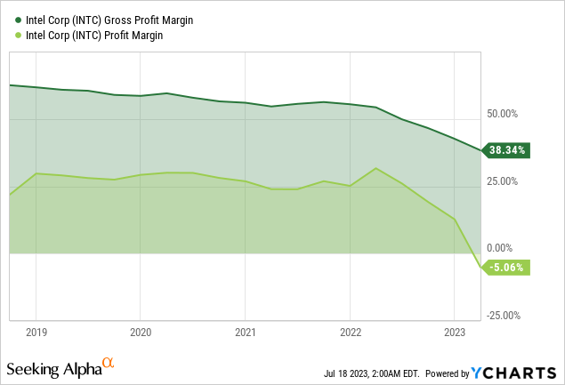
Intel has outlined a strategy to achieve cost savings of $8-$10 billion by the end of 2025. One of the critical factors in achieving this goal is transitioning to an internal foundry model, which will improve cost efficiency and increase long-term gross margin and operating margin.
To facilitate this, the company plans to report its internal foundry model’s profit and loss (P&L) separately rather than allocating costs to its business units. This approach aims to enhance transparency, accountability, and benchmarking against competitors, prompting the manufacturing organization and business units to prioritize cost efficiency and make better economic decisions. The internal foundry model will also reduce risks for external customers by leading the development of NextGen technology with its internal CPU.
Implementing the reportable P&L segment for the internal foundry model will encourage improved economic decision-making between the business and manufacturing units. Previously, business units could request expedited services from the manufacturing organization without much consideration for cost. While this expedited workflow benefited the business units by speeding up design processes, it created an 8-10% burden on manufacturing operations.
By establishing a stand-alone business group, the manufacturing organization will be able to charge 1.5-3x times the regular price for expedited requests, increasing accountability and reducing the overall number of such requests. Other identified areas for cost savings include reducing test sort times, adjusting ramp rates, optimizing product architecture, and managing sample production. Finally, these initiatives are expected to generate cost savings of $4-$5 billion over time.
Takeaway
Intel has shown its dedication to driving semiconductor innovation by retiring from chip generation-based development teams, focusing on technology modules, and adopting ground-breaking technologies like RibbonFET and PowerVia. These initiatives, along with the IDM 2.0 strategy and cost-cutting measures, put Intel in a position to compete effectively, draw in outside clients, and spur future growth in the semiconductor sector.
Editor’s Note: This article discusses one or more securities that do not trade on a major U.S. exchange. Please be aware of the risks associated with these stocks.
Analyst’s Disclosure: I/we have a beneficial long position in the shares of INTC, TSM either through stock ownership, options, or other derivatives. I wrote this article myself, and it expresses my own opinions. I am not receiving compensation for it (other than from Seeking Alpha). I have no business relationship with any company whose stock is mentioned in this article.
Seeking Alpha’s Disclosure: Past performance is no guarantee of future results. No recommendation or advice is being given as to whether any investment is suitable for a particular investor. Any views or opinions expressed above may not reflect those of Seeking Alpha as a whole. Seeking Alpha is not a licensed securities dealer, broker or US investment adviser or investment bank. Our analysts are third party authors that include both professional investors and individual investors who may not be licensed or certified by any institute or regulatory body.
Author of Yiazou Capital Research
Unlock your investment potential through deep business analysis.
I am the founder of Yiazou Capital Research, a stock-market research platform designed to elevate your due diligence process through in-depth analysis of businesses.
I have previously worked for Deloitte and KPMG in external auditing, internal auditing, and consulting.
I am a Chartered Certified Accountant and an ACCA Global member, and I hold BSc and MSc degrees from leading UK business schools.
In addition to my research platform, I am also the founder of a private business.

