Summary:
- KLA designs and sells “metrology and inspection” equipment, which plays a crucial role in yield enhancement for semiconductor manufacturing.
- KLA reported higher than expected EPS and revenue for Q3 2024.
- KLA holds a dominant market position in the metrology/inspection sector with a greater than 55% share.
- KLA is expected to benefit from increasing demand for advanced process control solutions for sub-5nm node chip production.

DNY59
One of the key issues about KLA (NASDAQ:KLAC) is that it is not like any of the other major equipment companies, and therefore any competitive analysis with them is pointless. Specifically, KLAC designs and sells “metrology and inspection” equipment. These are very different from the “processing” equipment from companies including Applied Materials (AMAT), Lam Research (LRCX), or Tokyo Electron (OTCPK:TOELY).
Significant differences for KLA are:
- Inspection Systems: By identifying and classifying defects during production, KLA’s inspection systems can pinpoint sources of yield loss and enable manufacturers to implement corrective measures.
- Metrology Solutions: Metrology data are used to monitor variations in process parameters, which can then be used to improve yield by ensuring dimensional accuracy and uniformity.
Importantly, KLA’s equipment plays a crucial role in yield enhancement for semiconductor manufacturing. Their inspection systems can detect and classify defects at various stages of production, allowing manufacturers to identify and address issues that could impact yield. KLA’s advanced analytics and data management software help in analyzing the collected data to optimize process parameters and improve overall yield.
As an example, Taiwan Semiconductor (TSM) reported a yield rate of 55% at 3nm for its 3NB process (and 63% for its 3NE process), meaning that nearly half of the wafers produced at its 3nm process will be categorized as a bad cassette batch of 25 wafers, representing a loss of $239,000 per cassette.
For the third quarter of 2024, KLA reported EPS of $5.26. This exceeded the analyst estimate of $5.01. KLA’s revenue for the same period stood at $2.36 billion, surpassing the analyst estimate by 2.16%.
Guidance for the fourth quarter of fiscal 2024 ending in June is that total revenue is expected to be in a range of $2.50 billion +/- $125 million, vs. $2.43B consensus.
Dominance in Metrology And Outperforming Peers
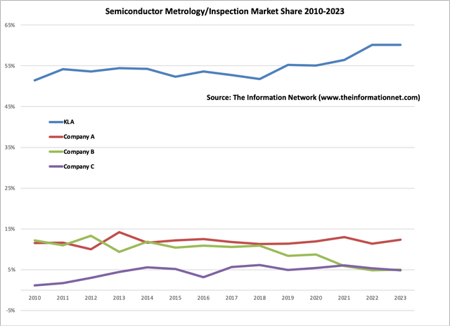
KLAC’s dominance in the process control sector extends to other competitors, as shown in Chart 1, according to The Information Network’s report entitled Metrology, Inspection, and Process Control in VLSI Manufacturing. Market share is a percentage of the overall global process control market.
Data show dominant market share for KLAC compared to Applied Materials, ASML (ASML), and Hitachi High Tech (HHT). Between 2010 and 2023, no competitor garnered more than 15% in a given year, as illustrated in Chart 1.
The Information Network
Chart 1
According to The Information Network’s above-mentioned report, there are three major segments comprising the $12 billion Metrology/Inspection market:
- Wafer Inspection/Defect Review
- Lithography Metrology
- Thin Film Metrology
Not only is KLAC a dominant leader in the overall metrology/inspection sector of the WFE semiconductor equipment market, the company also has a dominant market share in each of these segments.
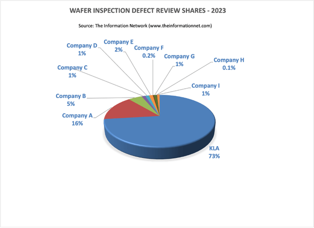
In Chart 2, I show that KLA had a 73% share of the Wafer Inspection/Defect Review segment. Compared to nine competitors, the largest share of a competitor was 16% in 2023.
The Information Network
Chart 3
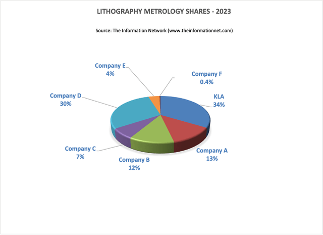
In Chart 4, I show that KLA had a 34% share of Lithography Metrology segment. Compared to six competitors, the largest share of a competitor was 30% in 2023.
The Information Network
Chart 4
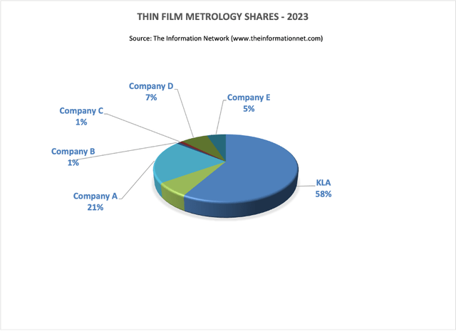
In Chart 5, I show that KLA had a 58% share of the Thin Film Metrology segment. Compared to five competitors, the largest share of a competitor was 21% in 2023.
The Information Network
Chart 5
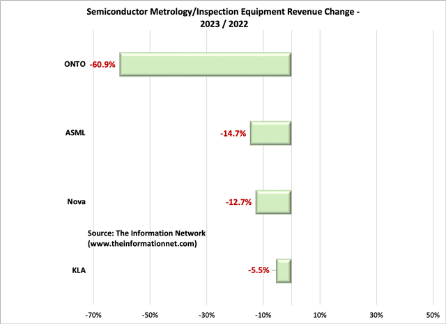
Chart 6 shows YoY wafer front end (WFE) semiconductor equipment revenue growth for 2023 vs 2022 based on a bottom-up analysis of all companies. This revenue growth is for semiconductor equipment only and does not include service, spare parts, or non-semiconductor business segments.
KLAC’s revenue grew -5.5%, outperforming the overall WFE semiconductor equipment market, which grew -9.0% to $86.6 billion in 2023, according to The Information Network’s report entitled “Global Semiconductor Equipment: Markets, Market Shares and Market Forecasts.”
The Information Network
Chart 6
Strong Growth From China
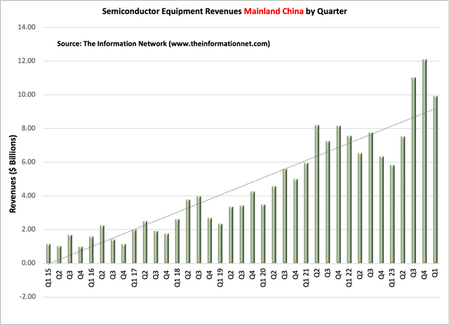
Chart 7 shows imports of equipment into China between Q1 2015 and Q1 2024. The trendline (green dotted line) shows consistently positive growth beginning in 2015, but hoarding of equipment by the Chinese for fear of further U.S. sanctions. This issue was also discussed in my January 3, 2024 article.
The Information Network
Chart 7
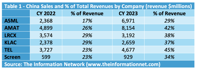
Table 1 shows China Sales by Equipment company to China in CY 2022 and 2023, as well as Q4 2023 and Q1 2024 for comparison. KLAC’s revenues from China increased to 38% of overall revenues to $2,659 million in 2023, up from 29% ($2,378 million) of total revenues in 2022.
The Information Network
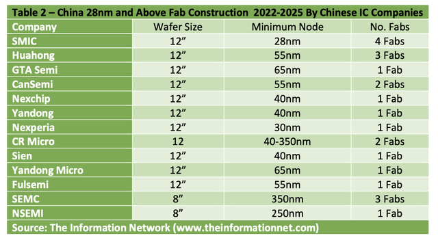
Table 2 shows planned fab construction in China between 2022 and 2025 for chip construction at the 28nm node and above, representing a significant tailwind for KLAC in China. These fabs are primarily foundries, a model that has been embraced in China because of the success of SMIC. Total fab spend is $67.566 billion.
The Information Network
Investor Takeaway
I have written in recent articles that equipment recovery will accelerate in 2H 2024.
According to Rick Wallace, president and CEO, KLA Corporation during the recent earnings call:
KLA’s March quarter results were above our adjusted guidance as customer demand and company execution tracked consistent with our expectations. As we have highlighted over the past few quarters, market conditions have stabilized and we expect our business levels to improve as we progress through the year. We are encouraged by the improvement in our customers’ businesses across multiple end markets and this improvement is translating into constructive discussions with our customers about future opportunities for leading edge capacity investments.
KLA holds a commanding position in the process control segment of the wafer fabrication equipment (WFE) industry, boasting a market share that is more than four times larger than its nearest competitor, Applied Materials.
This dominance is bolstered by the increasing complexity of semiconductor chips, which necessitates advanced process control solutions. As the industry shifts toward sophisticated architectures like chiplet-based designs, gate-all-around transistors, and high-bandwidth memory, the demand for KLA’s specialized equipment is expected to grow significantly.
The central focus of KLAC’s technology and products, as detailed above, is that by monitoring by inspection and metrology equipment, the more than 700 steps over three months to process a semiconductor wafers and device.
Importantly, KLA’s equipment plays a crucial role in yield enhancement for semiconductor manufacturing. Their inspection systems can detect and classify defects at various stages of production, allowing manufacturers to identify and address issues that could impact yield. KLA’s advanced analytics and data management software help in analyzing the collected data to optimize process parameters and improve overall yield.
Chart 8 shows my analysis of wafer ASPs (Average Selling Prices) by technology node. These ASPs increase with decreasing node. A 300mm wafer filled with 3nm node chips is priced at the foundry at $17,385, while a 28nm chip is priced at $5,670. The 3x price premium at 3nm means that any killer defects impacting the wafer yield will have a significantly greater financial impact at 3nm than 28nm.
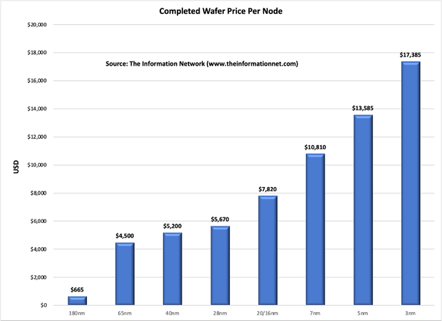
The Information Network
Chart 8
Wafers are processed in equipment one wafer at a time. Statistical process control (“SPC”) is defined as the use of statistical techniques to control a process or production method. SPC tools and procedures monitor process behavior, discover issues in internal systems, and find solutions for production issues. The combination of SPC and KLAC systems would enable the semiconductor manufacturer to stop production before the financial damage gets too great.
TSMC currently reports a yield rate of 55% at 3nm for its 3NB process (and 63% for its 3NE process), meaning that nearly half of the wafers produced at its 3nm process will be categorized as a bad cassette batch of 25 wafers, representing a loss of $239,000 per cassette.
I expect the yield rate to increase to a more normal 70% in 2Q 2024, benefitting from KLA equipment used for yield enhancement.
As companies ramp up production, yield increases. But if there is a catastrophic process failure, such as a process gas flow or contamination, it generates defects that need to be ascertained in a timely fashion.
As Best in Class, with a dominating share of equipment sales for sub 7nm chips, I rate KLAC a Strong Buy.
Editor’s Note: This article discusses one or more securities that do not trade on a major U.S. exchange. Please be aware of the risks associated with these stocks.
Analyst’s Disclosure: I/we have no stock, option or similar derivative position in any of the companies mentioned, and no plans to initiate any such positions within the next 72 hours. I wrote this article myself, and it expresses my own opinions. I am not receiving compensation for it (other than from Seeking Alpha). I have no business relationship with any company whose stock is mentioned in this article.
Seeking Alpha’s Disclosure: Past performance is no guarantee of future results. No recommendation or advice is being given as to whether any investment is suitable for a particular investor. Any views or opinions expressed above may not reflect those of Seeking Alpha as a whole. Seeking Alpha is not a licensed securities dealer, broker or US investment adviser or investment bank. Our analysts are third party authors that include both professional investors and individual investors who may not be licensed or certified by any institute or regulatory body.
This free article presents my analysis of this semiconductor equipment sector. A more detailed analysis is available on my Marketplace newsletter site Semiconductor Deep Dive. You can learn more about it here and start a risk free 2 week trial now.
